Boosting voltage converter DC DC. Switching Voltage Converters
Universal automobile converter (converter) "DC/DC".
This is a simple, versatile DC/DC converter (converter of one DC voltage to another). Its input voltage can be from 9 to 18 volts, with an output voltage of 5-28 volts, which can be changed from about 3 to 50 volts if necessary. The output voltage of this converter can be either less than the input, or more.
The power delivered to the load can reach up to 100 watts. The average converter load current is 2.5-3 amperes (depending on the output voltage, and with an output voltage of, for example, 5 volts, the load current can be 8 amperes or more).
This converter is suitable for various purposes, such as powering laptops, amplifiers, portable TVs and other household appliances from a 12V car on-board network, as well as charging mobile phones, USB devices, 24V appliances, etc.
The converter is resistant to overloads and short circuits at the output, since the input and output circuits are not galvanically connected to each other, and for example, the failure of the power transistor will not lead to the failure of the connected load, and only the voltage will disappear at the output (well, fuse blown).
Picture 1.
Converter circuit.
The converter is built on the UC3843 chip. Unlike conventional circuits of such converters, here, not a choke, but a transformer is used as an energy-producing element, with a ratio of turns of 1: 1, and therefore its input and output are galvanically isolated from each other.
The operating frequency of the converter is about 90-95 kHz.
The operating voltage of capacitors C8 and C9 is selected depending on the output voltage.
The value of the resistor R9 determines the current limiting threshold of the converter. The smaller its value, the greater the current limit.
Instead of the tuning resistor R3, you can put a variable one, and adjust the output voltage with it, or put a series of fixed resistors with fixed values of the output voltage, and select them with a switch.
To expand the output voltage range, it is necessary to recalculate the voltage divider R2, R3, R4, so that the voltage at pin 2 of the microcircuit is 2.5 volts at the required output voltage.

Figure 2.
Transformer.
The transformer core was used from computer power supplies AT, ATX, on which a DGS (group stabilization inductor) is wound. The color core is yellow-white, any suitable core can be used. Cores from similar power supplies and blue-green color are also well suited.
The windings of the transformer are wound in two wires and contain 2x24 turns, with a wire with a diameter of 1.0 mm. The beginning of the windings in the diagram are indicated by dots.
As output power transistors, it is desirable to use those with low open channel resistance. In particular SUP75N06-07L, SUP75N03-08, SMP60N03-10L, IRL1004, IRL3705N. And you still need to choose them with a maximum operating voltage, depending on the maximum output voltage. The maximum operating voltage of the transistor should not be less than 1.25 of the output voltage.
As a VD1 diode, you can use a coupled Schottky diode, with a reverse voltage of at least 40V and a maximum current of at least 15A, also preferably in the TO-220 package. For example SLB1640, or STPS1545, etc.
The circuit was assembled and tested on a breadboard. A field-effect transistor 09N03LA, torn from a "dead motherboard", was used as a power transistor. The diode is a coupled Schottky diode SBL2045CT.
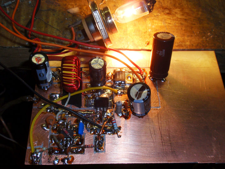
Figure 3
Test 15V-4A.
Testing the inverter with an input voltage of 12 volts and an output voltage of 15 volts. The inverter load current is 4 amps. Load power is 60 watts.

Figure 4
Test 5V-8A.
Testing the inverter with an input voltage of 12 volts, an output voltage of 5V and a load current of 8A. Load power is 40 watts. The power transistor used in the circuit = 09N03LA (SMD from the motherboard), D1 = SBL2045CT (from computer power supplies), R9 = 0R068 (0.068 Ohm), C8 = 2 x 4700 10V.
The printed circuit board designed for this device is 100x38 mm in size, taking into account the installation of a transistor and a diode on a radiator. Print in Sprint-Layout 6.0 format, attached in attachment.
Below in the photographs is an assembly option for this circuit using SMD components. Signet divorced for SMD components, size 1206.

Figure 5
Converter assembly option.
If there is no need to regulate the output voltage at the output of this converter, then the variable resistor R3 can be excluded, and the resistor R2 can be selected so that the output voltage of the converter corresponds to the required one.
Archive for article
As you know, white and blue LEDs need at least 3V to light up, unlike red LEDs which can glow from 1.2 to 1.5 volts depending on the type.
In order for the white LED to start glowing from one 1.5 volt battery, it is necessary to build an electronic circuit called. These devices are typically used to produce a higher voltage output compared to a direct current (DC) input.
In circuits with alternating current, this function. To get a higher output voltage, it is enough that the ratio of the number of turns of the secondary winding to the number of primary windings is greater than 1 (transformation ratio > 1).
Description of the operation of the converter for the LED
Returning to our DC/DC converter, there are many different options for implementing DC-DC conversion, many of which are quite complex. In our case, the goal is to create a simple and efficient converter circuit for stepping up the voltage from 1.5V to 3.5V. Below is a diagram of a similar DC-DC converter for LEDs.

To wind the inductor, ferrite is required, the shape and size of which can be any, but it is better to use a “ring” (or torus) core 1 ... 1.5 cm in diameter. This is usually used as a filter on power supply wires (black block next to the connector), it can also be found in switching power supplies, VCRs, scanners, etc. The winding is made with PEV-2 wire with a diameter of 0.4 mm and contains 30 turns.

The electronic circuit is very simple: it consists of a coil, two transistors, one capacitor and two resistors. The set is not impressive, but it does its job. The current consumption is 25 mA, which is equivalent to approximately 50 hours of continuous operation of an AA battery. The circuit works quite well, providing an average level of illumination of the LED.
Input voltages up to 61 V, output voltages from 0.6 V, output currents up to 4 A, the ability to externally synchronize and adjust the frequency, as well as adjust the current limit, adjust the soft start time, comprehensive load protection, a wide operating temperature range - all these features of modern sources power supplies are achievable with the new range of DC/DC converters manufactured by .
At the moment, the range of microcircuits of switching regulators manufactured by STMicro (Figure 1) allows you to create power supplies (PS) with input voltages up to 61 V and output currents up to 4 A.

The task of voltage conversion is not always easy. Each specific device has its own requirements for a voltage regulator. Sometimes price (consumer electronics), size (portable electronics), efficiency (battery-powered devices), or even speed of product development play a major role. These requirements often conflict with each other. For this reason, there is no ideal and universal voltage converter.
Currently, several types of converters are used: linear (voltage stabilizers), pulsed DC / DC converters, charge transfer circuits, and even power supplies based on galvanic isolators.
However, linear voltage regulators and step-down switching DC/DC converters remain the most common. The main difference between the functioning of these schemes can be seen from the name. In the first case, the power switch operates in a linear mode, in the second - in a key one. The main advantages, disadvantages and areas of application of these schemes are given below.
Features of the linear voltage regulator
The principle of operation of a linear voltage regulator is well known. The classic μA723 integrated stabilizer was developed back in 1967 by R. Widlar. Despite the fact that electronics have gone far ahead since then, the principles of operation have remained virtually unchanged.
The standard circuit of a linear voltage regulator consists of a number of basic elements (Figure 2): a power transistor VT1, a reference voltage source (ION), a compensation feedback circuit on an operational amplifier (op-amp). Modern regulators may contain additional functional blocks: protection circuits (from overheating, from overcurrent), power management circuits, etc.

The principle of operation of such stabilizers is quite simple. The feedback circuit on the op-amp compares the value of the reference voltage with the voltage of the output divider R1 / R2. At the output of the op amp, a mismatch is formed that determines the gate-source voltage of the power transistor VT1. The transistor operates in a linear mode: the higher the voltage at the output of the op-amp, the lower the gate-source voltage, and the greater the resistance VT1.
This circuit allows you to compensate for all changes in the input voltage. Indeed, suppose that the input voltage Uin has increased. This will cause the following chain of changes: Vin has increased → Vout will increase → the voltage at the divider R1/R2 will increase → the output voltage of the op-amp will increase → the “gate-source” voltage will decrease → the resistance VT1 will increase → Uout will decrease.
As a result, when the input voltage changes, the output voltage changes slightly.
When the output voltage decreases, reverse changes in the voltage values occur.
Features of the buck DC / DC converter
A simplified diagram of a classic DC/DC buck converter (type I converter, buck-converter, step-down converter) consists of several main elements (Figure 3): power transistor VT1, control circuit (CS), filter (Lf-Cf), reverse diode VD1.

Unlike the linear regulator circuit, the transistor VT1 operates in the key mode.
The cycle of operation of the circuit consists of two phases: the pump phase and the discharge phase (Figures 4…5).

In the pump phase, transistor VT1 is open and current flows through it (Figure 4). Energy is stored in the coil Lf and the capacitor Cf.

In the discharge phase, the transistor is closed, no current flows through it. Coil Lf acts as a current source. VD1 is a diode that is necessary for the reverse current to flow.
In both phases, a voltage is applied to the load equal to the voltage across the capacitor Cf.
The above circuit provides regulation of the output voltage when the pulse duration changes:
Uout = Uin × (ti/T)
If the value of the inductance is small, the discharge current through the inductance has time to reach zero. This mode is called the intermittent current mode. It is characterized by an increase in the current and voltage ripples on the capacitor, which leads to a deterioration in the quality of the output voltage and an increase in circuit noise. For this reason, the intermittent current mode is rarely used.
There is a kind of converter circuit in which the "inefficient" diode VD1 is replaced by a transistor. This transistor opens in antiphase with the main transistor VT1. Such a converter is called synchronous and has a higher efficiency.
Advantages and disadvantages of voltage conversion circuits
If one of the above schemes had absolute superiority, then the second one would be safely forgotten. However, this does not happen. This means that both schemes have advantages and disadvantages. The analysis of schemes should be carried out according to a wide range of criteria (Table 1).
Table 1. Advantages and disadvantages of voltage regulator circuits
| Characteristic | Linear Regulator | Step Down DC/DC Converter |
| Typical input voltage range, V | up to 30 | up to 100 |
| Typical output current range | hundreds of mA | units A |
| efficiency | short | high |
| Output voltage setting accuracy | units % | units % |
| Output voltage stability | high | average |
| Noise generated | short | high |
| The complexity of the circuit implementation | low | high |
| The complexity of the PCB topology | low | high |
| Price | low | high |
Electrical characteristics. For any converter, the main characteristics are efficiency, load current, input and output voltage range.

The efficiency value for linear regulators is small and inversely proportional to the input voltage (Figure 6). This is due to the fact that all the "extra" voltage drops on the transistor operating in linear mode. The power of the transistor is released as heat. Low efficiency leads to the fact that the range of input voltages and output currents of the linear regulator is relatively small: up to 30 V and up to 1 A.
The efficiency of a switching regulator is much higher and less dependent on the input voltage. At the same time, input voltages of more than 60 V and load currents of more than 1 A are not uncommon.
If a synchronous converter circuit is used, in which the inefficient freewheeling diode is replaced by a transistor, then the efficiency will be even higher.
Output voltage accuracy and stability. Linear stabilizers can have extremely high accuracy and parameter stability (fractions of a percent). The dependence of the output voltage on the change in the input voltage and on the load current does not exceed a few percent.
The switching regulator, according to the principle of operation, initially has the same sources of error as the linear regulator. In addition, the magnitude of the flowing current can significantly affect the deviation of the output voltage.
Noise characteristics. The linear regulator has a moderate noise characteristic. There are low-noise precision regulators used in high-precision measurement technology.
The switching regulator itself is a powerful source of interference, since the power transistor operates in the key mode. The generated interference is divided into conductive (transmitted through power lines) and inductive (transmitted through non-conductive media).
Conducted interference is eliminated with low-pass filters. The higher the operating frequency of the converter, the easier it is to get rid of interference. In measuring circuits, a switching regulator is often used in conjunction with a linear stabilizer. In this case, the level of interference is significantly reduced.
Getting rid of the harmful effects of inductive interference is much more difficult. This interference occurs in the inductor and is transmitted through air and non-conductive media. To eliminate them, shielded inductances, coils on a toroidal core are used. When laying out the board, a solid ground polygon fill is used and / or even a separate layer of ground is isolated in multilayer boards. In addition, the pulse converter itself is maximally removed from the measuring circuits.
Operational characteristics. From the point of view of simplicity of circuit implementation and PCB layout, linear regulators are extremely simple. In addition to the integrated regulator itself, only a couple of capacitors are required.
A switching converter will require at least an external L-C filter. In some cases, an external power transistor and an external flyback diode are required. This leads to the need for calculations and modeling, and the topology of the printed circuit board becomes much more complicated. An additional complication of the board occurs due to the requirement for EMC.
Price. Obviously, due to the large number of external components, the pulse converter will have a large cost.
As a conclusion, it is possible to determine the preferred areas of application for both types of converters:
- linear regulators can be applied in low power low voltage circuits with high accuracy, stability and low noise requirements. An example would be measurement and precision circuits. In addition, the small size and low cost of the final solution can be ideal for portable electronics and budget devices.
- Switching regulators are ideal for high power low and high voltage circuits in automotive, industrial and consumer electronics. The high efficiency often makes the use of DC/DC uncontested for portable and battery-powered devices.
Sometimes it becomes necessary to use linear regulators at high input voltages. In such cases, you can use stabilizers manufactured by STMicroelectronics, which have operating voltages of more than 18 V. (Table 2).
Table 2. STMicroelectronics High Input Voltage Linear Regulators
| Name | Description | Uin max, V | Uout nom, V | Iout nom, A | own fall, in |
| 35 | 5, 6, 8, 9, 10, 12, 15 | 0.5 | 2 | ||
| 500 mA Precision Regulator | 40 | 24 | 0.5 | 2 | |
| 2 A regulator | 35 | 0.225 | 2 | 2 | |
| , | Adjustable regulator | 40 | – | 0.1; 0.5; 1.5 | 2 |
| 3 A regulator | 20 | – | 3 | 2 | |
| 150mA Precision Regulator | 40 | – | 0.15 | 3 | |
| KFxx | 20 | 2.5: 8 | 0.5 | 0.4 | |
| Ultra-low self-drop regulator | 20 | 2.7: 12 | 0.25 | 0.4 | |
| 5A Regulator with Low Self-Drop and Adjustable Output Voltage | 30 | – | 1.5; 3; 5 | 1.3 | |
| lexx | Ultra-low self-drop regulator | 20 | 3; 3.3; 4.5; 5; 8 | 0.1 | 0.2 |
| Ultra-low self-drop regulator | 20 | 3.3; 5 | 0.1 | 0.2 | |
| Ultra-low self-drop regulator | 40 | 3.3; 5 | 0.1 | 0.25 | |
| 85 mA regulator with low self-drop | 24 | 2.5: 3.3 | 0.085 | 0.5 | |
| Precision Negative Voltage Regulator | -35 | -5; -8; -12; -15 | 1.5 | 1.1; 1.4 | |
| Negative voltage regulator | -35 | -5; -8; -12; -15 | 0.1 | 1.7 | |
| Adjustable Negative Voltage Regulator | -40 | – | 1.5 | 2 |
If a decision is made to build a pulsed IP, then a suitable converter chip should be selected. The choice is made taking into account a number of basic parameters.
Main characteristics of step-down pulsed DC/DC converters
We list the main parameters of pulse converters.
Input voltage range (V). Unfortunately, there is always a limitation not only on the maximum, but also on the minimum input voltage. The value of these parameters is always chosen with some margin.
Output voltage range (V). Due to the limitation on the minimum and maximum pulse duration, the range of output voltage values is limited.
Maximum output current (A). This parameter is limited by a number of factors: the maximum allowable power dissipation, the final value of the resistance of power switches, etc.
Converter operating frequency (kHz). The higher the conversion frequency, the easier it is to filter the output voltage. This allows you to deal with interference and reduce the values of the elements of the external L-C filter, which leads to an increase in output currents and to a decrease in size. However, an increase in the conversion frequency increases the switching losses of power switches and increases the inductive component of interference, which is clearly undesirable.
Efficiency (%) is an integral indicator of efficiency and is given in the form of graphs for various voltages and currents.
Other parameters (channel resistance of integrated power switches (mΩ), self-consumption current (μA), case thermal resistance, etc.) are less important, but they should also be taken into account.
New converters manufactured by STMicroelectronics have high input voltage and efficiency, and their parameters can be calculated using the free program eDesignSuite.
Switching DC/DC line from ST Microelectronics
The portfolio of DC/DC STMicroelectronics is constantly expanding. New converter chips have an extended input voltage range up to 61 V ( / ), high output currents, output voltages from 0.6 V ( / / ) (table 3).
Table 3. New DC/DC STMicroelectronics
| Characteristics | Name | |||||||
| L7987; L7987L | ||||||||
| Frame | VFQFPN-10L | HSOP-8; VFQFPN-8L; SO8 | HSOP-8; VFQFPN-8L; SO8 | HTSSOP16 | VFQFPN-10L; HSOP 8 | VFQFPN-10L; HSOP 8 | HSOP 8 | HTSSOP 16 |
| Input voltage Uin, V | 4.0…18 | 4.0…18 | 4.0…18 | 4…38 | 4.5…38 | 4.5…38 | 4.5…38 | 4.5…61 |
| Output current, A | 4 | 3 | 4 | 2 | 2 | 3 | 3 | 2 (L7987L); 3 (L7987) |
| Output voltage range, V | 0.8…0.88×Uin | 0.8…Uin | 0.8…Uin | 0.85…Uin | 0.6…Uin | 0.6…Uin | 0.6…Uin | 0.8…Uin |
| Operating frequency, kHz | 500 | 850 | 850 | 250…2000 | 250…1000 | 250…1000 | 250…1000 | 250…1500 |
| External frequency synchronization (max), kHz | No | No | No | 2000 | 1000 | 1000 | 1000 | 1500 |
| Functions | Smooth start; current overload protection; overheat protection | |||||||
| Additional functions | ENABLE; PGOOD | ENABLE | LNM; LCM; INHIBIT; overvoltage protection | ENABLE | PGOOD; protection against voltage dips; cutoff current adjustment | |||
| Chip operating temperature range, °C | -40…150 | |||||||
All new switching converter chips have the functions of soft start, overcurrent protection and overtemperature protection.
A powerful and fairly good voltage boost converter can be built on the basis of a simple multivibrator.
In my case, this inverter was built just to review the work, a small video was also made with the operation of this inverter.
About the circuit as a whole - a simple push-pull inverter, it's hard to imagine. The master oscillator and at the same time the power part are powerful field-effect transistors (it is desirable to use keys like IRFP260, IRFP460 and similar) connected according to the multivibrator circuit. As a transformer, you can use a ready-made trance from a computer power supply (the largest transformer).
For our purposes, it is necessary to use 12 volt windings and a midpoint (spit, tap). At the output of the transformer, the voltage can reach up to 260 volts. Since the output voltage is variable, it must be rectified with a diode bridge. It is desirable to assemble the bridge from 4 separate diodes, ready-made diode bridges are designed for mains frequencies of 50Hz, and in our circuit the output frequency is around 50kHz.
Be sure to use pulse, fast or ultra-fast diodes with a reverse voltage of at least 400 Volts and with a permissible current of 1 Amp and Above. You can use diodes MUR460, UF5408, HER307, HER207, UF4007, and others.
I recommend using the same diodes in the driving circuit circuit.
The inverter circuit works on the basis of parallel resonance, therefore, the frequency of operation will depend on our oscillatory circuit - in the face of the primary winding of the transformer and the capacitor in parallel with this winding.
At the expense of power and work in general. A properly assembled circuit does not need additional adjustment and works immediately. During operation, the keys should not heat up at all if the transformer output is not loaded. The idle current of the inverter can reach up to 300mA - this is the norm, higher is already a problem.
With good switches and a transformer, you can easily remove power in the region of 300 watts from this circuit without any problems, in some cases even 500 watts. The input voltage rating is quite high, the circuit will work from a source of 6 volts to 32 volts, I did not dare to supply more.
Chokes - wound with a 1.2mm wire on yellow-white rings from a group stabilization choke in a computer power supply. The number of turns of each inductor is -7, both inductors are completely identical.
Capacitors in parallel with the primary winding can heat up a little during operation, so I advise you to use high-voltage capacitors with an operating voltage of 400 volts and higher.
The circuit is simple and fully functional, but despite the simplicity and accessibility of the design, this is not an ideal option. The reason is not the best field key management. The circuit lacks a dedicated oscillator and drive circuit, making it not entirely reliable if the circuit is designed to operate continuously under load. The circuit can power LDS and devices that have built-in SMPS.
An important link is the transformer, which must be well wound and correctly phased, because it plays a major role in the reliable operation of the inverter.
Primary winding 2x5 turns with a bus of 5 wires 0.8 mm. The secondary winding is wound with 0.8 mm wire and contains 50 turns - this is in the case of self-winding of the transformer.