What does Vt mean in the diagram? Designation of radio components on the diagram. Elements of electrical circuit diagrams
Almost all electronic equipment, all radio electronics and electrical engineering products manufactured by industrial organizations and enterprises, home craftsmen, young technicians and radio amateurs, contain a certain amount of various purchased electronic components and elements produced mainly by domestic industry. But recently there has been a tendency to use electronic components and components of foreign production. These include, first of all, PPPs, capacitors, resistors, transformers, chokes, electrical connectors, batteries, HIT, switches, installation products and some other types of electronic devices.
The purchased components used or self-manufactured electrical electronic components are necessarily reflected in the circuit and installation electrical diagrams of devices, in drawings and other technical documentation, which are carried out in accordance with the requirements of ESKD standards.
Particular attention is paid to electrical circuit diagrams, which determine not only the basic electrical parameters, but also all the elements included in the device and the electrical connections between them. To understand and read electrical circuit diagrams, you must carefully familiarize yourself with the elements and components included in them, know exactly the scope of application and the principle of operation of the device in question. As a rule, information about the electrical power used is indicated in reference books and specifications - a list of these elements.
The connection between the list of ERE components and their graphic symbols is carried out through positional designations.
To construct conventional graphic symbols of ERE, standardized geometric symbols are used, each of which is used separately or in combination with others. Moreover, the meaning of each geometric image in a symbol in many cases depends on what other geometric symbol it is used in combination with.
The standardized and most frequently used graphic symbols of ERE in electrical circuit diagrams are shown in Fig. 1. 1. These designations apply to all components of the circuits, including electrical components, conductors and connections between them. And here the condition for the correct designation of the same type of electronic components and products becomes of utmost importance. For this purpose, positional designations are used, a mandatory part of which is the letter designation of the type of element, the type of its design and the digital designation of the ERE number. The diagrams also use an additional part of the ERE position designation, indicating the function of the element, in the form of a letter. The main types of letter designations for circuit elements are given in Table. 1.1.
Designations on drawings and diagrams of elements of general use refer to qualification ones, establishing the type of current and voltage. type of connection, control methods, pulse shape, type of modulation, electrical connections, direction of current transmission, signal, energy flow, etc.
Currently, the population and the trading network are using a significant number of various electronic instruments and devices, radio and television equipment, which are manufactured by foreign companies and various joint-stock companies. In stores you can purchase various types of ERI and ERI with foreign designations. In table 1. 2 provides information about the most common ERE of foreign countries with the corresponding designations and their domestically produced analogues.
This is the first time this information has been published in such a volume.
1- pnp structure transistor in a housing, general designation;
2- transistor of n-p-n structure in the housing, general designation,
3 - field-effect transistor with p-n junction and n channel,
4 - field-effect transistor with p-n junction and p channel,
5 - unijunction transistor with n-type base, b1, b2 - base terminals, e - emitter terminal,
6 - photodiode,
7 - rectifier diode,
8 - zener diode (avalanche rectifier diode) one-sided,
9 - thermal-electric diode,
10 - diode dinistor, lockable in the opposite direction;
11 - zener diode (diodolavin rectifier) with bidirectional conductivity,
12 - triode thyristor;
13 - photoresistor;
14 - variable resistor, rheostat, general designation,
15 - variable resistor,
16 - variable resistor with taps,
17 - trimming resistor-potentiometer;
18 - thermistor with positive temperature coefficient of direct heating (heating),
19 - varistor;
20 - constant capacitor, general designation;
21 - polarized constant capacitor;
22 - oxide polarized electrolytic capacitor, general designation;
23 - constant resistor, general designation;
24 - constant resistor with a rated power of 0.05 W;
25 - constant resistor with a rated power of 0.125 W,
26 - constant resistor with a rated power of 0.25 W,
27 - constant resistor with a rated power of 0.5 W,
28 - constant resistor with a rated power of 1 W,
29 - constant resistor with a rated dissipation power of 2 W,
30 - constant resistor with a rated dissipation power of 5 W;
31 - constant resistor with one symmetrical additional tap;
32 - constant resistor with one asymmetrical additional tap;

Fig 1.1 Symbols of graphical symbols of electrical power in electrical, radio and automation circuits
33 - non-polarized oxide capacitor;
34 - feed-through capacitor (the arc indicates the housing, the external electrode);
35 - variable capacitor (arrow indicates rotor);
36 - trimming capacitor, general designation;
37 - varicond;
38 - noise suppression capacitor;
39 - LED;
40 - tunnel diode;
41 - incandescent lighting and signal lamp;
42 - electric bell;
43 - galvanic or battery element;
44 - electrical communication line with one branch;
45 - electrical communication line with two branches;
46 - a group of wires connected to one electrical connection point. Two wires;
47 - four wires connected to one electrical connection point;
48 - battery made of galvanic cells or rechargeable battery;
49 - coaxial cable. The screen is connected to the body;
50 - winding of a transformer, autotransformer, choke, magnetic amplifier;
51 - working winding of the magnetic amplifier;
52 - control winding of the magnetic amplifier;
53 - transformer without a core (magnetic core) with permanent connection (the dots indicate the beginning of the windings);
54 - transformer with a magnetodielectric core;
55 - inductor, choke without magnetic circuit;
56 - single-phase transformer with a ferromagnetic magnetic core and a screen between the windings;
57 - single-phase three-winding transformer with a ferromagnetic magnetic core with a tap in the secondary winding;
58 - single-phase autotransformer with voltage regulation;
59 - fuse;
60 - fuse switch;
61 - fuse-disconnector;
62 - detachable contact connection;
63 - amplifier (the direction of signal transmission is indicated by the top of the triangle on the horizontal communication line);
64 - detachable contact connection pin;

Fig 1.1 Symbols of graphical symbols of electronic electrical power in electrical, radio and automation circuits
65 - detachable contact connection socket,
66 - contact for removable connection, for example using a clamp
67 - contact of a permanent connection, for example, made by soldering
68 - single-pole push-button switch with self-resetting closing contact
69 - breaking contact of the switching device, general designation
70 - closing contact of the switching device (switch, relay), general designation. Single pole switch.
71 - switching device contact, general designation. Single pole double throw switch.
72- three-position switching contact with neutral position
73 - normally open contact without self-return
74 - push-button switch with normally open contact
75 - push-button pull-out switch with normally open contact
76 - push-button switch with button return,
77 - push-button pull-out switch with normally open contact
78 - push-button switch with return by pressing the button a second time,
79 - electric relay with normally open and switching contacts,
80 - relay polarized for one direction of current in a winding with a neutral position
81 - relay polarized for both directions of current in a winding with a neutral position
82 - electrothermal relay without self-reset, with return by pressing the button again,
83 - detachable single-pole connection
84 - socket of five-wire contact connector
85 - pin of contact detachable coaxial connection
86 - contact connection socket
87 - four-wire connection pin
88 - four-wire connection socket
89 - jumper switching breaking circuit
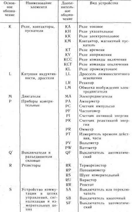
Table 1.1. Letter designations of circuit elements

Continuation of Table 1.1

We continue to get acquainted with semiconductor devices and with this article we will begin to deal with transistor. In this part we will get acquainted with device and marking of bipolar transistors.
Semiconductor transistors come in two types: bipolar And field.
Unlike field-effect transistors, bipolar ones are most widely used in radio electronics, and in order to somehow distinguish these transistors from each other, bipolar ones are usually called simply transistors.
1. Design and designation of a bipolar transistor.
Schematically, a bipolar transistor can be represented as a plate with alternating regions different electrical conductivity, which form two p-n junctions. And both extreme areas have electrical conductivity of the same type, and average area with electrical conductivity of a different type, and where each of the areas has mine contact pin.

If in the extreme regions of the semiconductor the hole electrical conductivity, and in the middle region electronic, then such a semiconductor device is called a structure transistor p-n-p.
And if in the extreme regions it prevails electronic electrical conductivity, and on average hole, then such a transistor has the structure n-p-n.

Now let’s take the schematic part of the transistor and cover any extreme area, for example, the area collector, and look at the result: we still have open areas bases And emitter, that is, the result is a semiconductor with one p-n junction or an ordinary semiconductor diode. You can read about diodes.

If we cover the area emitter, then the areas will remain open bases And collector- and you also get a diode.
This leads to the conclusion that a bipolar transistor can be represented as two diodes with one general area included towards each other. In this case, the general (middle) area is called base, and the areas adjacent to the base collector And emitter. These are the three electrodes of the transistor.

The areas adjacent to the base are made unequal: one of the areas is made so that it most effectively produces input(injection) of charge carriers to the database, and the other area is made in such a way that it is effectively carried out conclusion(extraction) of charge carriers from the database.
From here it turns out:
input(injection) of charge carriers into the base is called emitter emitter.
area of the transistor whose purpose is conclusion(extraction) of carriers from the database is called collector, and the corresponding p-n junction collector.
That is, it turns out that the emitter enters electric charges into the base, and the collector picks up.
The difference in the designations of transistors of different structures on circuit diagrams lies only in the direction arrows emitter: in p-n-p in transistors it faces towards the base, and in n-p-n transistors - from the base.
2. Manufacturing technology of bipolar transistors.
The manufacturing technology of transistors is no different from the manufacturing technology of diodes. Even in the initial period of development of transistor technology, bipolar transistors were made only from germanium using the fusion impurities, and such transistors are called alloy.

A crystal of germanium is taken and pieces of indium are melted into it.
Indium atoms diffuse(penetrate) into the body of a germanium crystal, forming two regions in it p-type– collector and emitter. Between these areas there remains a very thin (several microns) layer of semiconductor n-type, which is called the base. And in order to protect the crystal from the influence of light and mechanical stress, it is placed in a metal-glass, metal-ceramic or plastic case.
The picture below shows the schematic device and design alloy transistor assembled on a metal disk with a diameter of less than 10 mm. A crystal holder is welded to the top of this disk, which is the internal lead of the base, and at the bottom of the disk is its outer wire lead.

The internal terminals of the collector and emitter are welded to conductors, which are soldered into glass insulators and serve as the external terminals of these electrodes. The metal cap protects the device from light and mechanical damage. This is how the most common low-power low-frequency germanium transistors from the MP37 - MP42 series are designed.

In the designation, the letter “M” indicates that the transistor body cold welded, the letter “P” is the first letter of the word “ planar", and the numbers mean the serial serial number of the transistor. As a rule, after the serial number the letters A, B, C, D, etc. are placed, indicating the type of transistor in this series, for example, MP42B.
With the advent of new technologies, they learned to process silicon crystals, and based on it they created silicon transistors, which have received the most widespread use in radio engineering and today have almost completely replaced germanium devices.

Silicon transistors can operate at higher temperatures (up to 125ºC), have lower collector and emitter reverse currents, and higher breakdown voltages.
The main method of manufacturing modern transistors is planar technology, and transistors made using this technology are called planar. For such transistors, the p-n junctions emitter-base and collector-base are in the same plane. The essence of the method is diffusion(melting) into a wafer of initial silicon an impurity, which can be in the gaseous, liquid or solid phase.
As a rule, the collector of a transistor made using this technology is a wafer of original silicon, on the surface of which melted two balls of impurity elements close to each other. During heating to a strictly defined temperature, diffusion impurity elements into the silicon wafer.

In this case, one ball forms a thin basic area, and the other emitter. As a result, in the original silicon wafer, two p-n junctions forming a p-n-p structure transistor. The most common silicon transistors are manufactured using this technology.
Also, for the manufacture of transistor structures, combined methods are widely used: fusion and diffusion or a combination of different diffusion options (double-sided, double-sided). A possible example of such a transistor: the base region can be diffusion, and the collector and emitter can be alloy.
The use of a particular technology in the creation of semiconductor devices is dictated by various considerations related to technical and economic indicators, as well as their reliability.
3. Marking of bipolar transistors.
Today, the marking of transistors, according to which they are distinguished and produced in production, consists of four elements.
For example: GT109A, GT328, 1T310V, KT203B, KT817A, 2T903V.
The first element is a letter G, TO, A or number 1 , 2 , 3 – characterizes the semiconductor material and the temperature conditions of the transistor.
1
. Letter G or number 1
assigned germanium transistors;
2
. Letter TO or number 2
assigned silicon transistors;
3
. Letter A or number 3
assigned to transistors whose semiconductor material is gallium arsenide.
The number instead of the letter indicates that this transistor can operate at elevated temperatures: germanium - above 60ºС, and silicon - above 85ºС.
The second element is a letter T from the initial word "transistor".
The third element is a three-digit number from 101 before 999 – indicates the serial serial number of the development and the purpose of the transistor. These parameters are given in the transistor reference book.
The fourth element is the letter from A before TO– indicates the type of transistors of this series.

However, you can still find transistors that have an earlier designation system, for example, P27, P213, P401, P416, MP39, etc. Such transistors were produced back in the 60s and 70s before the introduction of modern labeling of semiconductor devices. These transistors may be outdated, but they are still popular and used in amateur radio circuits.
In this part of the article, we examined only general methods for manufacturing transistor structures, so that it would be easier for a novice radio amateur to understand the internal structure of a transistor.
We will finish here, and then we will conduct several experiments and, based on them, draw practical conclusions about operation of a bipolar transistor.
Good luck!
Literature:
1. Borisov V.G - Young radio amateur. 1985
2. Pasynkov V.V., Chirkin L.K. - Semiconductor devices: Textbook. for universities for special purposes “Semiconductors and dielectrics” and “Semiconductor and microelectronic devices” - 4th ed. reworked and additional 1987

On circuit diagrams you can find designations for a field-effect transistor of one type or another.
In order not to get confused and to get the most complete idea of what kind of transistor is used in the circuit, let’s compare the conventional graphic designation of a unipolar transistor and its distinctive properties and features.
Regardless of the type of field-effect transistor, it has three terminals. One of them is called Gate(Z). The gate is the control electrode; control voltage is applied to it. The next output is called Source(AND). The source is similar to the emitter of bipolar transistors. The third output is called Stock(WITH). The drain is the terminal from which the output current is removed.
On foreign electronic circuits you can see the following designation of the terminals of unipolar transistors:
G- shutter (from English - G ate "shutter", "gate");
S– source (from English – S ource "source", "beginning");
D– stock (from English – D rain “outflow”, “leakage”).
Knowing the foreign designations of the field-effect transistor terminals, it will be easy to understand the circuits of imported electronics.
Designation of a field-effect transistor with a control p-n junction (J-FET).
So. A transistor with a control p-n junction is designated in the diagrams as follows:

n-channel J-FET

p-channel J-FET
Depending on the type of carriers that are used to form the conductive channel (the area through which regulated current flows), these transistors can be n-channel or p-channel. The graphic designation shows that n-channels are depicted with an arrow pointing inward, and p-channels pointing outward.
Designation of MOS transistor.
Unipolar MIS-type transistors (MOSFETs) have a slightly different graphic designation than J-FETs with a control p-n junction. MOSFETs can also be either n-channel or p-channel.
MOSFETs exist in two types: built-in channel And induced channel.
What is the difference?
The difference is that the induced channel transistor turns on only when a positive or only negative threshold voltage is applied to the gate. Threshold voltage ( U por ) is the voltage between the gate and source terminals at which the field-effect transistor opens and drain current begins to flow through it ( Ic ).
The polarity of the threshold voltage depends on the type of channel. For p-channel mosfets, a negative “-” voltage must be applied to the gate, and for those with an n-channel, a positive “+” voltage must be applied. Mosfets with an induced channel are also called transistors. enriched type. Therefore, if you hear people talking about an enriched type mosfet, you should know that this is a transistor with an induced channel. Its symbol is shown below.

n-channel MOSFET

p-channel MOSFET
The main difference between an MOS transistor with an induced channel and a field-effect transistor with a built-in channel is that it opens only at a certain value (U threshold) of a positive or negative voltage (depending on the type of channel - n or p).
A transistor with a built-in channel opens already at “0”, and with a negative voltage at the gate it operates lean mode(also open, but passes less current). If a positive “+” voltage is applied to the gate, it will continue to open and go into the so-called enrichment mode- the drain current will increase. This example describes the operation of an n-channel mosfet with a built-in channel. They are also called transistors lean type. The following shows their conventional representation in the diagrams.


On the conventional graphic designation, you can distinguish a transistor with an induced channel from a transistor with a built-in channel by the break in the vertical line.
Sometimes in technical literature you can see an image of a MOS transistor with a fourth terminal, which is a continuation of the arrow line indicating the type of channel. So, the fourth output is the substrate output. This image of a mosfet is used, as a rule, to describe a discrete (i.e., separate) transistor and is used only as a visual model. During the manufacturing process, the substrate is usually connected to the source terminal.

MOSFET with substrate lead

Designation of a power MOSFET transistor
As a result of connecting the source and substrate in the field mosfet structure, a built-in diode. This diode does not affect the operation of the device, since it is connected in the reverse direction to the circuit. In some cases, the built-in diode, which is formed due to the technological features of manufacturing a power MOSFET, can be used in practice. In the latest generations of power MOSFETs, the built-in diode is used to protect the element itself.

The built-in diode may not be indicated on the symbol of a powerful MOS transistor, although in reality such a diode is present in any powerful field device.
Reading diagrams is impossible without knowledge of the conventional graphic and letter designations of the elements. Most of them are standardized and described in regulatory documents. Most of them were published in the last century, and only one new standard was adopted, in 2011 (GOST 2-702-2011 ESKD. Rules for the execution of electrical circuits), so sometimes a new element base is designated according to the principle “as who came up with it.” And this is the difficulty of reading circuit diagrams of new devices. But, basically, the symbols in electrical circuits are described and are well known to many.
Two types of symbols are often used on diagrams: graphic and alphabetic, and denominations are also often indicated. From this data, many can immediately tell how the scheme works. This skill is developed over years of practice, and first you need to understand and remember the symbols in electrical circuits. Then, knowing the operation of each element, you can imagine the final result of the device.
Drawing and reading different diagrams usually require different elements. There are many types of circuits, but in electrical engineering the following are usually used:

There are many other types of electrical circuits, but they are not used in home practice. The exception is the route of cables passing through the site and the supply of electricity to the house. This type of document will definitely be needed and useful, but it is more of a plan than an outline.
Basic images and functional features
Switching devices (switches, contactors, etc.) are built on contacts of various mechanics. There are make, break and switch contacts. The normally open contact is open; when it is switched to operating state, the circuit is closed. The break contact is normally closed, but under certain conditions it operates, breaking the circuit.

The switching contact can be two or three position. In the first case, first one circuit works, then another. The second one has a neutral position.
In addition, contacts can perform different functions: contactor, disconnector, switch, etc. All of them also have a symbol and are applied to the corresponding contacts. There are functions that are performed only by moving contacts. They are shown in the photo below.

Basic functions can only be performed by fixed contacts.

Symbols for single line diagrams
As has already been said, single-line diagrams indicate only the power part: RCDs, automatic devices, automatic circuit breakers, sockets, circuit breakers, switches, etc. and connections between them. The designations of these conventional elements can be used in electrical panel diagrams.
The main feature of graphic symbols in electrical circuits is that devices similar in principle of operation differ in some small detail. For example, a machine (circuit breaker) and a switch differ only in two small details - the presence/absence of a rectangle on the contact and the shape of the icon on the fixed contact, which display the functions of these contacts. The only difference between a contactor and a switch designation is the shape of the icon on the fixed contact. It's a very small difference, but the device and its functions are different. You need to look closely at all these little things and remember them.

There is also a small difference between the symbols of the RCD and the differential circuit breaker. It also only functions as moving and fixed contacts.
The situation is approximately the same with relay and contactor coils. They look like a rectangle with small graphic additions.

In this case, it’s easier to remember, since there are quite serious differences in the appearance of the additional icons. With a photo relay it’s so simple - the rays of the sun are associated with the arrows. A pulse relay is also quite easy to distinguish by the characteristic shape of the sign.

A little easier with lamps and connections. They have different “pictures”. A detachable connection (such as a socket/plug or socket/plug) looks like two brackets, and a detachable connection (such as a terminal block) looks like circles. Moreover, the number of pairs of checkmarks or circles indicates the number of wires.
Picture of buses and wires
In any circuit there are connections and for the most part they are made by wires. Some connections are buses - more powerful conductor elements from which taps can extend. Wires are indicated by a thin line, and branches/connections are indicated by dots. If there are no points, it is not a connection, but an intersection (without an electrical connection).

There are separate images for buses, but they are used if they need to be graphically separated from communication lines, wires and cables.

On wiring diagrams it is often necessary to indicate not only how the cable or wire runs, but also its characteristics or installation method. All this is also displayed graphically. This is also necessary information for reading drawings.
How switches, switches, sockets are depicted
There are no standards-approved images for some types of this equipment. So, dimmers (light regulators) and push-button switches remained without designation.
But all other types of switches have their own symbols in electrical diagrams. They come in open and hidden installations, respectively, there are also two groups of icons. The difference is the position of the line on the key image. In order to understand in the diagram what type of switch we are talking about, this must be remembered.
There are separate designations for two-key and three-key switches. In the documentation they are called “twin” and “twin”, respectively. There are differences for cases with different degrees of protection. In rooms with normal operating conditions, switches with IP20, maybe up to IP23, are installed. In wet rooms (bathroom, swimming pool) or outdoors, the degree of protection should be at least IP44. Their images differ in that the circles are filled in. So it's easy to distinguish them.

There are separate images for the switches. These are switches that allow you to control turning the light on/off from two points (there are also three, but without standard images).
The same trend is observed in the designations of sockets and socket groups: there are single, double sockets, and there are groups of several pieces. Products for rooms with normal operating conditions (IP from 20 to 23) have an unpainted middle; for wet rooms with a housing of increased protection (IP44 and higher), the middle is tinted dark.

Symbols in electrical diagrams: sockets of different types of installation (open, hidden)
Having understood the logic of the designation and remembering some initial data (what is the difference between the symbolic image of an open and hidden installation socket, for example), after a while you will be able to confidently navigate the drawings and diagrams.
Lamps on diagrams
This section describes the symbols in the electrical circuits of various lamps and fixtures. Here the situation with the designations of the new element base is better: there are even signs for LED lamps and fixtures, compact fluorescent lamps (housekeepers). It’s also good that the images of lamps of different types differ significantly - it’s difficult to confuse them. For example, lamps with incandescent lamps are depicted in the form of a circle, with long linear fluorescent lamps - a long narrow rectangle. The difference in the image of a linear fluorescent lamp and an LED lamp is not very big - only dashes at the ends - but even here you can remember.

The standard even includes symbols in electrical diagrams for ceiling and pendant lamps (socket). They also have a rather unusual shape - circles of small diameter with dashes. In general, this section is easier to navigate than others.
Elements of electrical circuit diagrams
Schematic diagrams of devices contain a different element base. Communication lines, terminals, connectors, light bulbs are also depicted, but in addition, there is a large number of radio elements: resistors, capacitors, fuses, diodes, thyristors, LEDs. Most of the symbols in the electrical circuits of this element base are shown in the figures below.


Rarer ones will have to be looked for separately. But most circuits contain these elements.
Letter symbols in electrical diagrams
In addition to graphic images, elements on the diagrams are labeled. It also helps to read the diagrams. Next to the letter designation of an element there is often its serial number. This is done so that later it is easy to find the type and parameters in the specification.

The table above shows international designations. There is also a domestic standard - GOST 7624-55. Excerpts from there with the table below.
